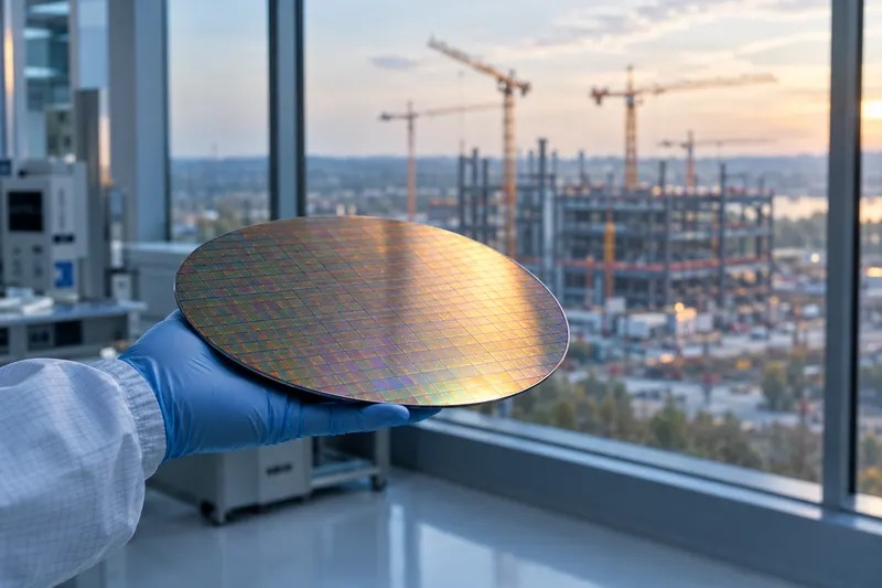
IBM plans to give outside chip designers early access to its nanostack architecture in the first quarter of 2027, roughly nine months after the company first showed it. The IBM 0.7nm chip remains a research project, and IBM has not named the manufacturer that would build it.
Those two facts define the story. The architecture is real and public, but it is still at the research stage, and the route from a design kit to a shipping product runs through partners that IBM has not yet identified.
What IBM is releasing and when
IBM says it will make an early research and development process design kit, or PDK, for its 7-angstrom nanostack technology available in the first quarter of 2027, according to IBM's research blog. Wccftech and Kantan News also reported the timeline.
A PDK packages the design rules, checking scripts and layout tools that engineers need to evaluate a process before it reaches production. A designer can draft circuits, run them through checks and see whether a layout is feasible without a wafer ever being made. For the people who build chips, that matters more than any headline transistor count.
Why the 0.7nm label is a name, not a measurement
Chip makers have named process generations with nanometer figures for decades. IBM now says those node names no longer map to exact physical dimensions. The 0.7nm label describes a manufacturing generation, not a literal feature size, as StorageReview reported.
Readers should treat the number as a position in a sequence of processes. The more useful yardsticks are density, performance and efficiency, and IBM has published figures for all three.
What the IBM 0.7nm chip packs in
IBM says the chip holds nearly 100 billion transistors on a die about the size of a fingernail. That is roughly twice the density of the 2nm chip the company unveiled in May 2021, as Forbes reported. IBM's design-kit post cites a die area of about 150 mm².
Dividing nearly 100 billion transistors by 150 square millimeters gives roughly 670 million transistors per square millimeter. A figure of 666 million per square millimeter has circulated in one analyst post, but it does not appear in any IBM primary source reviewed for this story, so treat it as unconfirmed.
Against the 2nm node, IBM cites up to 50% more performance or up to 70% greater energy efficiency, according to HPCwire. IBM also reports that SRAM, the cache memory built into processors, scales about 40%, a result presented at the VLSI 2026 symposium. These are research-stage figures from IBM, not measurements from a product customers can buy.
How stacking differs from shrinking
Conventional scaling has mostly meant making transistors smaller side to side. The nanostack design instead stacks and staggers nanosheet transistors vertically using 3D sequential integration, as TechTimes describes it. That approach adds a vertical dimension to the layout rather than squeezing the existing one.
IBM's research indicates the process works within a conventional 300 mm CMOS wafer line, according to HPCwire. That detail matters for factories, because a process that fits existing wafer tools is easier to adopt than one that requires new equipment. It does not mean any factory is ready to build it.
IBM framed the work in sweeping terms. In its June 25 press release, Jay Gambetta, director of IBM Research and an IBM Fellow, said "we're reinventing how chips are built." At the June press conference, Gambetta said "It's a meaningful leap forward," as MIT Technology Review reported.
The Siemens partnership is research, not a production deal
On October 14, IBM and Siemens announced a research collaboration. Siemens is contributing electronic design automation, process simulation, lithography optimization and manufacturing software to help IBM model and refine future nanostack generations, according to Bitcoinversus. The announcement is described as research, not a commercial production launch.
Most coverage of the Siemens deal comes from secondary aggregators, including a KuCoin flash news item. Check IBM's own release before repeating specifics. The direction is still informative. Design automation sits on the design side of the pipeline, while process simulation and lithography sit closer to manufacturing, so the collaboration spans both ends.
Where nanostack fits in IBM's nanosheet history
IBM unveiled its 2nm chip technology in May 2021, according to the IBM India newsroom. MIT Technology Review reports that IBM developed the nanosheet transistor design that current 2nm and 3nm chips use, and that Samsung, Intel and TSMC all rely on that approach. Reports disagree on when the nanosheet was invented, with some dating it to 2015 and others to 2017.
IBM does not manufacture commercial logic chips at volume. It develops architectures and licenses them to foundries and partners, including Samsung, Intel, TSMC and Japan's Rapidus, according to TechTimes. That model explains why IBM can announce a 0.7nm architecture without naming a customer. It also means IBM's influence depends on partners adopting its designs.
IBM's near-term focus, per TechTimes, is helping partners scale 2nm nanosheet chips. Nanostack is therefore a longer bet than the next product cycle. For American chip supply, the nearer-term capacity story sits elsewhere, including the GlobalFoundries Malta plan, which concerns manufacturing rather than architecture research.
Who gains, who waits and what to watch
US chip designers, including teams building AI accelerators, are the immediate audience for the kit. Early access in 2027 gives them time to test layouts before any production commitment exists. Chip buyers and cloud operators could eventually see denser AI hardware with better energy efficiency.
IBM's own timeline puts that at least several years away, and it projects production in as little as five years. No action is needed from consumers or IT teams right now. Investors and chip supply-chain professionals should watch for the following:
- A named foundry or manufacturer willing to commercialize nanostack, which IBM has not disclosed
- A commercialization timeline with dates beyond the first-quarter 2027 kit
- Whether the 2027 PDK is research-only or open to commercial chip designers
- The full Siemens terms in IBM's own release, rather than secondary summaries
- Independent testing of the performance and efficiency claims
The next concrete date is the first quarter of 2027. If the kit arrives on schedule and a manufacturer steps forward, the story moves from research demonstrations to test chips, and that is when the density and efficiency claims will face real measurement.